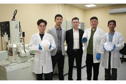
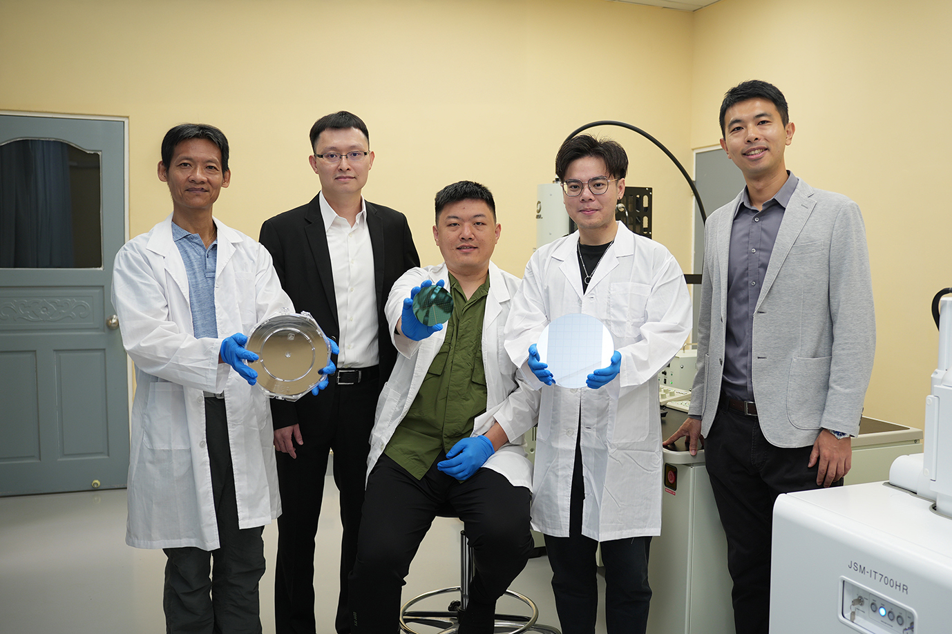
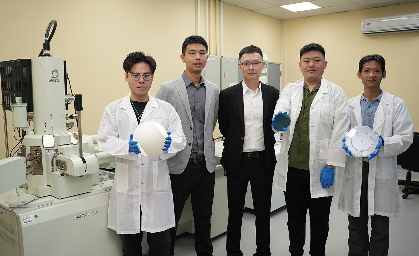
NCHU and NCKU Collaborate to Develop the World’s First Freestanding Ferroelectric 2D Transistor — Pioneering Innovation for Next-Generation AI Chips and Smart Technologies
2025-07-04
興新聞張貼者
Unit秘書室
1,446
With the support of Taiwan’s National Science and Technology Council and the Ministry of Education, a collaborative research team from National Chung Hsing University (NCHU) and National Cheng Kung University (NCKU) has achieved a significant breakthrough in semiconductor technology. Their pioneering work on a freestanding ferroelectric film integrated with a two-dimensional (2D) semiconductor transistor has been published in the prestigious journal Nature Electronics (June 2025). This milestone not only demonstrates Taiwan’s global competitiveness in advanced materials and nanoelectronics but also lays the foundation for future innovations in AI computing, memory integration, and 3D chip packaging.
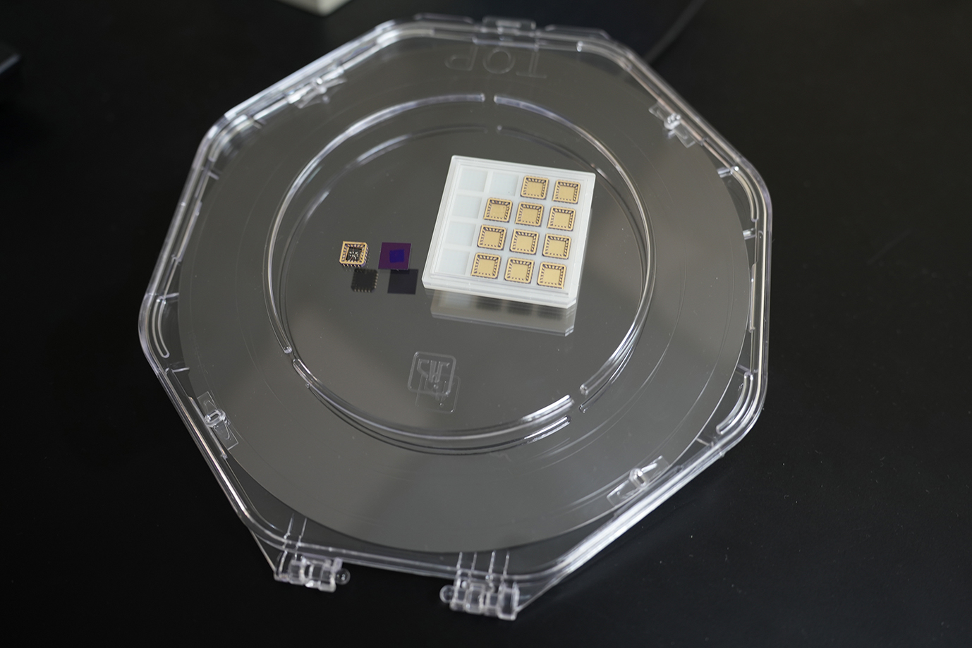
The research introduces the first-ever sub-20 nm ferroelectric Hf₀.₅Zr₀.₅O₂ (HZO) film that is both freestanding and transferable. By integrating this ultrathin film onto a MoS₂ 2D semiconductor, the team built a high-performance gate dielectric with ferroelectric and high-k properties, without harming the sensitive 2D interface. The resulting device achieved an outstanding on/off current ratio exceeding 10⁹ and a remarkably low subthreshold swing of just 53 mV/dec—both significantly surpassing current mainstream technologies.
While 2D materials are widely seen as promising options for next-generation transistors and memory devices, integrating high-quality dielectric or ferroelectric layers has long been challenging. Conventional methods like atomic layer deposition (ALD) and chemical vapor deposition (CVD) often harm the electronic properties of 2D materials and involve complex post-processing steps. This study tackles these issues with a new freestanding transfer technique, opening up new opportunities for interface engineering and low-power device designs.
Dr. Che-Yi Lin, a postdoctoral researcher at NCHU and one of the lead authors, emphasized: “This technology liberates ferroelectric materials from fixed silicon substrates, enabling their integration wherever needed, much like a transferable film. What’s more, we demonstrated real, working devices—not just materials—with practical applications in logic computing.”
At NCKU, Professor Jan-Chi Yang’s team, including Dr. Yu-Chen Liu and Po-Cia Chen, developed high-quality HZO films and transfer techniques. Prof. Yang noted: “Our goal was to make ferroelectric materials not only functional but also reconfigurable. This flexibility is key to enabling future logic, memory, and AI chip innovations.”
Under Professor Yen-Fu Lin's leadership at NCHU’s Department of Physics and Institute of Nanoscience, the team successfully demonstrated complete circuit functionality, including inverters, logic gates, and a 1-bit adder, even with a nanoscale channel length of 13 nm. “This is not just a material platform—it’s a fully functional, scalable device platform ready for integration into modern chip design,” Prof. Lin stated.
Looking ahead, the technology is expected to be scalable to 8-inch and 12-inch wafers using pulsed laser deposition (PLD), making it compatible with mainstream semiconductor fabrication lines. This innovation holds promise for a broad range of applications—from energy-efficient AI smartphones and durable wearable devices to real-time medical diagnostics and automotive electronics. As chips become more compact, intelligent, and energy-saving, the research brings us closer to a smarter, more connected, and more sustainable future.
https://www.nature.com/articles/s41928-025-01398-y
NCHU and NCKU Collaborate to Develop the World’s First Freestanding Ferroelectric 2D Transistor — Pioneering Innovation for Next-Generation AI Chips and Smart Technologies
NCHU and NCKU Collaborate to Develop the World’s First Freestanding Ferroelectric 2D Transistor — Pioneering Innovation for Next-Generation AI Chips and Smart Technologies